SIAE MICROELETTRONICA is very proud of its highly skilled RF design department and advanced laboratory facilities, with over 25 years experience in microwave circuits productions and high quality thin film customisations. This division is the leader in the production of ceramic, glass, quartz or nitride aluminium substrates using sputtering deposition.
RF Design Center
Our RF Component Design lab, is divided into two areas each with its own high technological expertise.
The first part is working on MCM (Multi Circuit Modules), designing PCB based modules like complete Rx receivers and Tx transmitters including the relevant local oscillators (L.O.).
The second group is dedicated to MMIC (Monolithic Microwave Integrated Circuits) designing components and micro circuitry based on Gallium Arsenide (GaAS ), Silicon Germanium (SiGe) and Gallium Nitride (GaN) technology. Those Designs are then used to develop the most cost effective, best integrated , and most stable circuits dedicated to the SIAE MICROELETTRONICA Microwave portfolio production. Modern Microwave units are high precision devices and their perfection comes from the best design, materials, components and precisely controlled production. The RF Components lab develops a wide variety of state-of-the-art components, the most advanced are listed below:
- Low Phase Noise VOCs (Voltage Controlled Oscillators)
- LNCs up to 80GHz (Low Noise down converters for high frequencies)
- VGAs (Variable Gain Amplifiers)
- PA (Power Amplifiers)
- Integrated IF circuits
- Highly integrated UP-converters and VGAs
and the most advanced “All inclusive” SIP (Systems in Package): a complex multi-element unique micro package containing what is needed to arrange a complete Transmitter and/or Receiver. The most advanced SIP covers the highest frequency transceivers usable in Microwave Telecommunications: V-Bands, E-Bands and W-Bands. The microwave SIPs are mounted on a single PCB allowing fast, easy and reliable implementation of a complete ODU.
Both areas make use of up-to date CAD platforms: ADS Agilent for 2D circuit designs and HFSS ANSYS for 3D modeling.
SIAE MICROELETTRONICA maintains the IPR, patents and copyrights of all our designs, however also offers and distributes under licence to third parties companies.
RF DESIGN CENTER
VCO, LNC, IF IC, Up & Down Converters all have a highly integrated functionality that have been internally designed using the most advanced semiconductor processes and CAE tools. Overall cost reduction, improved reliability and optimised performance are the driving factors for all of SIAE MICROELETTRONICA’s internal MMIC designs. Our ability to conduct the design phase internally enables an easier and faster transition from the prototyping phase to volume production thus reducing the time to market.
Manufacturing
Module assembly yields are particularly affected by the cleanliness of the parts to be put together, so that plasma cleaning of the printed substrate on which the devices should be attached is the first step in the manufacturing process.
The attachment is done through selective high precision dispensing of electrically/thermally conductive glue followed by the video controlled pick-and-place phase.
The achieved positioning accuracy is suitable for frequencies up to and above 100 GHz.
After the attachment phase, all modules are passed through a second, less aggressive, plasma cleaning to improve yield in the following step of wire bonding.
Typically only gold wires or gold ribbons are used with processes including ball-bonding through ribbon edge bonding.
The bond positioning to the relevant bonding pads is controlled by means of video pattern recognition.
To guarantee effectiveness of the bonding, an in line pull test is automatically performed daily at the beginning of every production cycle; furthermore each bonding is video inspected to monitor metal strain at the gold/gold interphase.
The manufacturing activity is completed with module cover positioning and sealing.
Under request the assembled modules can be in line 100% electrically tested. The passed units can be assembled in tape and reel for automatic installation in the final equipment.
MANUFACTURING
Manufacturing in the Technological Department (i.e. clean room area) is based on a modular assembly practice, starting with highly sophisticated automatic bare chip or packaged device attachment to the substrate (both ceramic or soft board) and relative high speed wire or ribbon bonding. For special applications, device attachment can be done through SnAu (or equivalent) eutectic alloy, the module can be hermetically sealed and subsequently 100% tested for gross and fine leakage.
Clean Room Processes
All the processes are rolled out in strictly controlled environments (class 10,000 clean rooms and class 100 laminar flow benches) in order to ensure the quality level of the nano-metric accuracy needed for high frequency Thin Film Technology. The Thin Film Technology process includes a multitude of refined steps starting from mask design to the final high quality components.
This process includes the following:
- Sputtering (Tantalum, Nickel, Palladium)
- Photolithography (UV based)
- Gold Electroplating
- Wet and Dry Etching
- Diamond Blade Circuit Dacing
- Chip and Wire process
The fully automated chip and wire process can guarantee micro-metric accuracy from glue dispensing, pick-and-place under video pattern recognition, and precision bonding suitable for applications up to W-Band.
CLEAN ROOM PROCESSES
The Thin Film Technology department, together with our RF Design labs, lead the technological advances made by SIAE MICROLETTRONICA. These divisions are expert in producing nano-metric precision components starting from ceramic, quartz or alluminium substrates. Those substrates become the foundation for building high quality components. SIAE MICROELETTRONICA produces all these product lines in house, including: RF filters, oscillators, and RF Tx/Rx modules. It is hard to imagine a more optimised process for providing high quality microwave equipment, than an integrated production line from substrate to radio terminal.
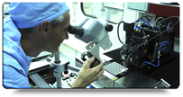
Clean Room Quality Control
The quality levels and the production yields are maintained through in-depth control of all parameters in the technological lines:
- Substrates Cleanliness : before and after sputtering process all substrates are plasma cleaned
- Components Cleanliness: before and after the chip and wire activities pieces are plasma cleaned
A dedicated quality procedure is applied to all of the activities of the technological department in order to ensure the correct accuracies required by the millimetric frequency applications of the V,E and W-bands are achieved:
- Nano-Metric accuracy for sputtered layers (one in five unit test)
- Micro-Metric accuracy for chip and wire process (100% inline dimension automatic test)
- Electrical performance test (100% inline for Tx/Rx and SIPs)
- Tape and Reel (all SIPs which passed relevant electrical tests are automatically tape and reel assembled)
CLEAN ROOM QUALITY CONTROL
A dedicated quality procedure is applied to all of the activities of the technological department in order to ensure the correct accuracies required by the millimetric frequency applications of the V,E,W-bands are achieved: Nano-Metric accuracy for sputtered layer (one in five unit test) Micro-Metric accuracy for chip and wire process (100% inline dimension automatic test) Electrical performance test (100% inline for Tx/Rx and SIPs) Tape and Reel (all SIPs which passed relevant electrical tests are automatically tape and reel assembled)